


 購物車 / 產生報價單




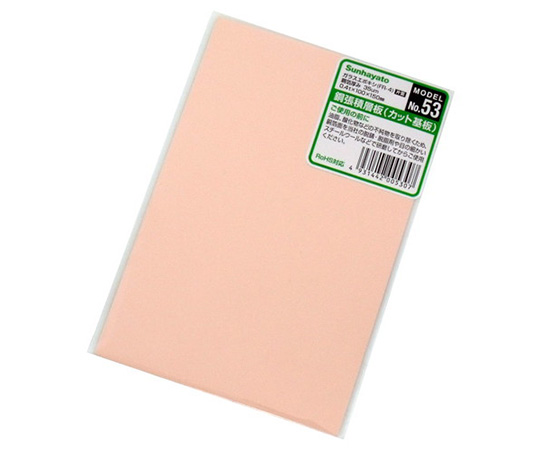
商品圖片僅供參考,選購時請再留意商品規格
Sunhayato Corp. 裁切式單面玻纖環氧樹脂銅箔基板 100 x 150 x 0.4 毫米 53
商品包含多種型號及規格,請點選「立即選購規格」挑選
💡 重要通知:
因中東戰爭造成原物料波動影響,若訂單成立後進貨成本發生重大異動,我們將主動聯繫您協商處理。造成不便,敬請見諒。

月結報帳 / 信用卡 / 銀行轉帳

宅配快速到貨,滿 NT$ 999 元即享免運!
選購型號
商品介紹
Features
- Material: Glass Epoxy (FR-4) One Side
- Thickness x Dimensions (mm): 0.4 x 100 x 150
- Copper foil thickness: 35 μm
- A circuit board is formed by directly transferring lettering tape to the copper foil surface and etching. ・0.4 mm thick copper clad laminate (cut substrate). ・It can be cut easily with scissors, so it can be processed into various shapes. ・Since the substrate bends, it can also fit along curved surfaces. ・It is also possible to form a multilayer substrate by bonding the etched substrates.
Package size
- 105x155x5mm
- 0.02kg
以上圖片及相關資訊由 AS ONE提供。
若有現場安裝、說明或特殊配送需求,歡迎事前與科研市集聯繫。部分商品因供應條件限制,可能無法提供相關服務,敬請見諒。